Time of Flight Secondary Ion Mass Spectrometry (TOF-SIMS)
Time of flight secondary ion mass spectrometry, or TOF-SIMS for short, is a surface-sensitive analytical method. The sample to be analyzed is scanned with a focused ion beam, whereby particles are released from the top layer of the material - including secondary ions, which are used in TOF-SIMS for analysis purposes. The detection itself takes place via a time of flight mass analyzer, which can record a complete mass spectrum during a sputter pulse.
In this way, the surfaces of solid bodies are examined for their chemical characteristics. Here, the composition of the sample surface is analyzed on an elementary and molecular level. This method also gives the possibility of a complete three-dimensional analysis of the sample. With TOF-SIMS, a large number of substances are suitable as sample material to be examined, such as semiconductors, polymers, paper, glass, ceramics and many more.
How does a TOF-SIMS system work
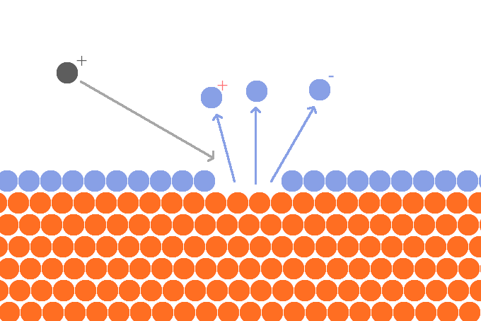
A pulsed primary beam with an energy of up to 30 keV is focused on a sample to be examined. Collisions (collision cascade) occur between the ions of the primary beam and the sample material (topmost monolayer), in which mainly neutral particles, but also negatively and positively charged particles are released. These charged particles are then accelerated towards the mass spectrometer in an electric field.
-

Schematic view of the interaction of primary ions with the sample monolayer in TOF-SIMS
The TOF-SIMS analysis of charged particles takes advantage of the fact that ions with the same energy but different masses move at different speeds. Lighter ions have higher velocities and reach the detector faster than heavier ions. Measuring the time of flight of a particle makes it possible to determine its mass.
Basic structure of a time of flight secondary ion mass spectrometer
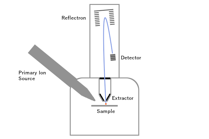
A TOF-SIMS system basically consists of the components
- Ion beam column with a pulsed primary ion beam
- Sample stage
- Electron flood gun for charge compensation
- Time of Flight Mass Spectrometer (TOF Analyzer)
-

Basic structure of TOF-SIMS: column of primary ion beam, sample, extractor, reflectron, detector
Ion beam column with a pulsed primary ion beam
The ion beam column basically consists of four sections, which can be logically divided into the ion source, the electrostatic beam shaping, the blanking/pulsing of the beam and the final beam shaping (focusing on the sample).
The ion source can consist of a liquid metal ion source (LMIS). Depending on the manufacturer, different materials are used, such as bismuth (Bi). Gas cluster ion sources with argon are also used.
The beam is formed by apertures, electrostatic Einzel lenses and quadrupoles. The pulsing of the primary ion beam is achieved by an electrostatic blanker. The final beam shaping, which focuses the ion beam onto the sample, is in turn achieved using a special Einzel lens as well as quadrupoles and octupoles. Here applies the rule: the smaller the beam diameter, the better the spatial resolution.
TOF-SIMS sample stage
Sample holders for TOF-SIMS applications can usually be moved in the five axes X, Y, Z as well as R (rotation) and T (tilt). The sample table is at the ground potential of the system.
Electron flood gun for charge compensation
In the case of non-conductive material, sputtering on the sample surface can lead to the issue, that the grounding via the sample holder cannot be used for charge compensation. When the material is bombarded by ions, more charged particles are brought onto the sample than are sputtered out. This can lead to potential is building up. This charge disrupts the process and therefore it is necessary to dissipate the potential with an Electron Flood Gun.
The Electron Flood Gun comes into play after each cycle, which includes a pulse of the primary ion beam and the subsequent extraction of the secondary ions. In this way, charges can be compensated. Negative effects of an excess of electrons are neutralized with a so-called extraction bias voltage.
Time of Flight Mass Spectrometer (TOF Analyzer)
The actual spectrometer of the TOF-SIMS consists of an extractor that accelerates the secondary ions from the sample towards the detector. In the ideal case, the secondary ions have the same kinetic energy when they traverse the field-free space. The analysis is based on a different mass to charge ratio (m/z ratio). The intensity of the detected signal as a function of the flight time makes it possible to make a statement about the nuclide or isotope proportions in the sample (provided the detector is calibrated).
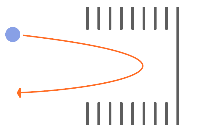
Since it is not possible under real conditions for all secondary ions to have exactly the same energy, a reflectron is used in TOF-SIMS, for example. The reflectron is an electrostatic mirror into which ions penetrate and are then reflected to the detector. Higher energy secondary ions have a longer trajectory as they penetrate deeper into the reflectron. Ions with lower energy are reflected faster and have a shorter trajectory to the TOF-SIMS detector. Thanks to this device, all ions of the same mass arrive at the detector at the same time.
-

Schematic example for a TOF-SIMS reflectron
TOF-SIMS operating modes
Time of flight secondary ion mass spectrometers can be used in different operating modes. Four of the most popular modes are described below.
Surface spectrometry
The goal of surface spectrometry is usually to study the original composition of the surface. Since SIMS is usually a destructive method, a low dose for the primary ions must be used for analysis purposes.
For this purpose, the TOF-SIMS is operated as a static SIMS, which means that only the top monolayers of the sample are touched and major destruction is avoided. The ion currents achieved are low, but detailed elementary and molecular information can be obtained. This method has a sensitivity in the ppm/ppb range.
Surface Imaging/Mapping
In surface imaging, the sample surface to be examined is scanned with a finely focused ion beam. Similar to an electron microscope, an image can be obtained that provides information about the mass distribution of the secondary ions and is suitable for chemical mapping of the surface.
Depth profiling
When analyzing depth profiles, the TOF-SIMS works in dual-beam mode. One ion beam is used to analyze the surface and the second ion beam is used to produce a sputter crater.
Sputtering is done with a reactive ion beam consisting of, for example, oxygen (O2) or cesium (Cs). The use of clusters is also possible. The energy of these ion beams is low to achieve higher sensitivity and high depth resolution.
3D analysis
The 3D analysis using TOF-SIMS is a combination of the operating modes spectrometry, imaging and depth profiling. With the help of this examination, complex and unknown structures and defects can be analyzed.
Possible material samples for TOF-SIMS analysis
A time of flight secondary ion mass spectrometer allows the investigation of a large number of different materials. These can be both electrically conductive and insulating and include biomaterials, glass, pharmaceuticals, coatings, semiconductors and polymers, among others.
Applications for TOF-SIMS spectrometers
The large number of materials that can be examined also provides a large number of possibilities for the application of TOF-SIMS spectrometers.
Detection of trace metals
In the semiconductor industry, it is becoming increasingly important to detect trace metals in semiconductors. TOF-SIMS spectrometers are particularly well suited for this because they are also able to detect light elements and their isotopes.
Contamination of semiconductors
With a TOF-SIMS spectrometer it is possible to detect inorganic and organic impurities in semiconductors. Such contamination can occur during the production process through contact with gloves or tools. The impurities in the clean room can also settle on the semiconductors. Ultimately, as a result of their further chemical processing, semiconductors are in direct contact with undesirable substances in the end product.


