Scanning electron microscope (SEM)
A scanning electron microscope is a microscope that uses a beam of electrons to scan an object (sample) in a specific pattern. The sample and the electron beam interact with each other so that, among other things, secondary electrons (SE) are generated, which are detected by a corresponding detector and then processed into an image. The generated image contains information about the sample surface.
Basic structure and functional principle of an SEM microscope
The electron beam in a scanning electron microscope is generated by an electron source. In simple SEM microscopes, the source is a tungsten hairpin cathode, or LaB6, or in more expensive instruments, a thermal field emission gun (FEG). The thermal field emission cathode (Schottky emitter) is actively heated and thus has a higher beam intensity. The work function of the electrons at the cathode tip is reduced by the zirconium oxide coating. The electron source is always in ultra-high vacuum (UHV).
By applying an acceleration voltage, the electrons generated at the source are accelerated in the direction of the sample. Common acceleration voltages for scanning electron microscopes are between 100 V and 30 kV. On their way to the sample, the electrons are deflected or bundled by mostly electromagnetic lenses. Apertures are used to shape the main electron beam and filter out spurious effects.
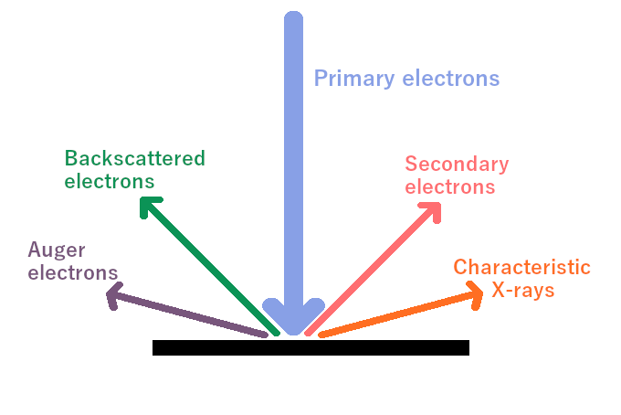
A beam of electrons that pass through the column and hits the sample (primary electrons) causes an interaction in the material. A result of these interactions can be secondary electrons, back-scattered electrons, Auger electrons or characteristic X-ray radiation.
-

Schematic view of the electron beam interactions in the SEM microscope
Secondary electrons in the scanning electron microscope
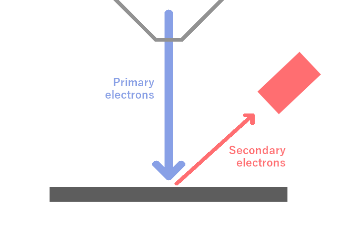
The secondary electrons (SE) are most commonly used in scanning electron microscopes. They are detected for imaging by Everhart-Thornley detectors or so-called inlens detectors. The low energy of these electrons is used in the SEM microscope to image the topography of the sample. The detector only picks up secondary electrons that come from the surface area down to a depth of a few nanometers. Lower-lying electrons no longer leave the sample.
The image contrast depends on many variables, surfaces that are inclined towards the detector can appear brighter than surfaces that are turned away or shaded. Furthermore, the number of secondary electrons that are formed depends on the material and the possible charging of a sample also has a major influence on the image contrast.
-

Schematic view of secondary electrons in the scanning electron microscope
Back-scattered electrons in the scanning electron microscope
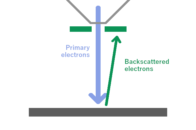
Back-scattered electrons (BSE) are often used in scanning electron microscopes. The primary electrons that are scattered back from the sample and have a higher energy than secondary electrons are detected. Material contrasts can be imaged particularly well with a BSE detector, since the backscattering on the sample surface largely depends on the atomic number of the material. This is visible in the BSE image by different brightness contrasts, which indicate heavier or lighter elements.
-

Schematic view of back-scattered electrons in the scanning electron microscope


